In the ever-evolving landscape of technology, the demand for faster, more efficient circuit boards has driven the innovation of High-Density Interconnect (HDI) PCBs. These advanced circuit boards are a pivotal departure from conventional single-layer PCBs, offering a leap in component density and paving the way for smaller, more powerful electronic devices. In this comprehensive guide, we will delve into the intricacies of HDI PCBs, exploring their advantages, common applications, layer stackup, and essential design tips. Additionally, we will examine why HDI PCBs are crucial for the future of electronic design.
Understanding High-Density Interconnect PCBs
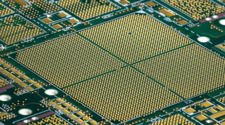
HDI PCBs stand out for their multilayered structure, differing significantly from the single-layer PCBs that have been prevalent for years. While conventional PCBs typically have one layer, HDI boards can range from two to five layers, with three and four-layer configurations being the most common. Each layer is intricately printed with conductive tracks, facilitating the flow of current between components on different layers.
The primary motivation behind the adoption of HDI PCB lies in their ability to accommodate more components on a single board. This breakthrough enables the creation of smaller and more efficient devices while maintaining, and often enhancing, performance levels. HDI PCBs have found widespread applications across various industries, with a notable surge in popularity within the data storage market due to the imperative of storing information in progressively shrinking dimensions.
Advantages of HDI PCBs
Reduced Space Requirements:
- HDI PCBs excel in situations where space is a premium. When coupled with technologies like 3D stacking or interposers, these boards require less physical space than traditional PCBs. This makes them ideal for compact devices such as smartphones and tablet computers.
Higher Throughput:
- The manufacturing and assembly processes for HDI boards are streamlined, leading to faster processing times compared to traditional boards. Reduced handling and sorting contribute to a lower risk of damage or misalignment during production.
Better Quality Control:
- The simplified manufacturing process of HDI PCBs results in fewer opportunities for human error during production and assembly. This enhances overall quality control and ensures a more reliable final product.
Lower Failure Rate:
- The materials used in HDI boards boast a longer life cycle than those in traditional PCBs. This increased durability translates to a lower failure rate, making HDI PCBs a more robust and reliable choice.
Common Applications of HDI PCBs
HDI PCBs find application in diverse industries, with certain sectors leveraging their capabilities more prominently. Some notable applications include:
Automotive Electronics:
- Used in sensors and actuators controlling functions like steering, braking, and acceleration in automobiles.
Industrial Control Panels and Automation Systems:
- Employed in the creation of reliable industrial control panels and automation systems for applications in medical equipment, power plants, oil refineries, and other critical industrial facilities.
Telecommunications Equipment:
- Widely utilized in high-performance and cost-effective telecommunications equipment such as routers, switches, and servers.
Medical Equipment:
- Integral to medical imaging systems like X-ray machines, MRI scanners, and various diagnostic equipment such as blood analyzers.
HDI PCB Layer Stackup
The layer stackup of an HDI PCB is a critical aspect of its design, influencing performance and functionality. A typical HDI PCB stackup includes four main layers:
Copper Layer (Layer 1):
- The primary layer where signal traces, power, and ground connections are routed. Vias are strategically placed on this layer to facilitate connections between layers.
Ground Plane (Layer 2):
- A single-sided copper layer serving as a large surface for heat dissipation. It also acts as a barrier, preventing signal interference.
Signal Layer (Layer 3):
- Dedicated to housing all signal traces, with each row typically corresponding to a component pin. Each row has its ground plane on both sides.
Component Pads (Top and Bottom, Layer 4):
- The component pads connect to corresponding vias on Layer 1 and corresponding pads on Layer 3 through openings in the solder mask.
Design Tips for HDI PCBs
Minimize Solder Mask Thickness:
- To increase component density, reduce the solder mask thickness. This can be achieved by resizing artwork or utilizing a smaller solder mask font.
Use High-Density Vias (HDV):
- Implement high-density vias to improve signal integrity, especially in high-frequency signals (more details). HDV provides better impedance matching between layers and can be used for both through holes or blind vias.
Design with Multiple Ground Planes:
- Incorporate multiple ground planes to facilitate efficient signal routing, enhance signal integrity, and reduce crosstalk between signals. This also ensures better impedance matching between layers.
The Future Significance of HDI PCBs
Looking ahead, HDI PCBs are poised to play a pivotal role in shaping the future of electronic design. As technological advancements continue at an unprecedented pace, the demand for smaller, more efficient, and high-performance electronic devices is on the rise. HDI PCBs offer a scalable solution, allowing designers to maximize component density, minimize footprint, and enhance overall system performance.
Innovations in fields such as Internet of Things (IoT), wearable technology, and miniaturized medical devices rely heavily on the capabilities of HDI PCBs. The ability to pack more functionality into compact spaces aligns with the evolving needs of modern applications. From smart wearable devices to advanced medical implants, HDI PCBs provide the foundation for pushing the boundaries of what is possible in electronics.
Moreover, the push for sustainability and energy efficiency in electronics amplifies the importance of HDI PCBs. As devices become smaller and more power-efficient, the environmental impact is reduced, contributing to a greener and more sustainable technological landscape.
Take Home
High-Density Interconnect PCBs represent not only the present but also the future of electronic design. With their ability to address the demand for smaller, more efficient devices across various industries, HDI PCBs have become an indispensable component in the technological evolution. As we embrace the era of interconnected devices, IoT, and advanced medical technologies, the significance of HDI PCBs will only continue to grow. For those seeking high-quality HDI PCBs, manufacturers like Hemeixin offer cutting-edge solutions, ushering in a new era of electronic innovation. As the electronic landscape evolves, HDI PCBs stand as a testament to the relentless pursuit of efficiency and compact design in the realm of technology, ensuring that the future is both powerful and sustainable.
Last Updated: February 7, 2024


